Inners preparation before Multilayer lamination
Here we are again to continue our virtual factory tour to better understand all process steps necessary to produce PCBs.
After inner’s automatic optical inspection (AOI) inners are subject to
- punching and
- copper surface preparation
Inner layers are punched to obtain the registration holes necessary to grant the inner layers to be aligned to each-others after pressing. The operator loads each inner into the punching machine which, through an optical system, lines up the inner itself and punches the registration holes.
Inner layers are printed with a "predictive" distortion to the nominal values: indeed, during the pressing phase inner layers slightly change their size because of temperature and pressure and depending on base material and copper percentage mainly; and these changes need to be managed: we work at the level of micron, "prediction" couldn't be "gut feeling", printing distortions are based on years and years of experience.
The shape of the registration holes is also important to avoid any rotation of the inner layers between each other during the pressing phase.
As we already said PCB manufacturing requires a wide range of competence where chemical and mechanical are often mixed.
After punching inner layers are ready for copper surface preparation before pressing.
The main objective of this phase is to make the copper surface "rough" enough to guarantee the best possible adhesion with pre-preg during pressing so to avoid one of the most critical risks in PCBs: the delamination.
Copper preparation is performed through a chemical process typically named black-oxide by the technicians: it is in fact based on the oxidation of copper surface that changes from bright to blacked. This change corresponds to the roughness acquisition by the copper surface.
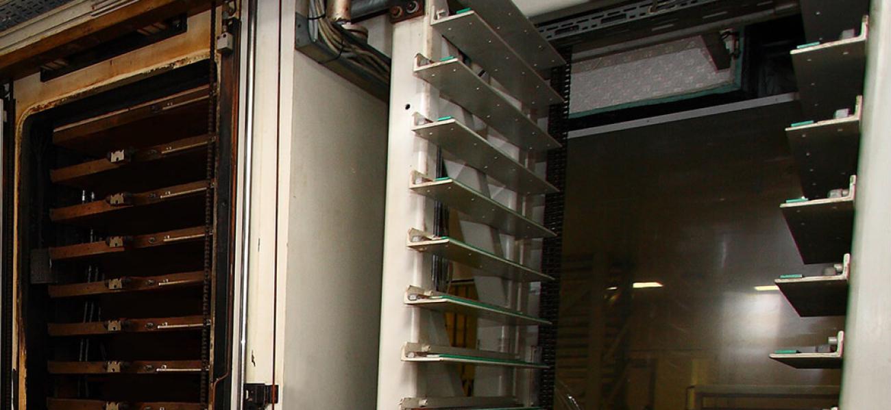
An additional phase to avoid the risk of delamination is to make on inner layers a baking after the black-oxide process. This thermal process guarantees the moisture to evacuate from the inner layers.
Vaporization of moisture during pressing could be responsible to avoid the correct bonding between the resin of the pre-preg with the inner layers or with the copper foil on which outer layers will be “drawn”.
Delamination could show its presence later after pressing in the shape of "bubbles" on copper foil or even later after outer layer's etching resulting in "whitened spots or patches" on the PCB surface; or in the shape of pink ring "defect" as a local delamination at the inner‐layer oxide interfaces around drilled holes that become evident after dissolution of the oxide during plating processes.
That’s why a correct copper surface preparation coupled with moisture absence are “a must” to avoid delamination.
If you want to learn more about the PCB manufacturing process, feel free to contact us!