Vias technologies
Vias technologies

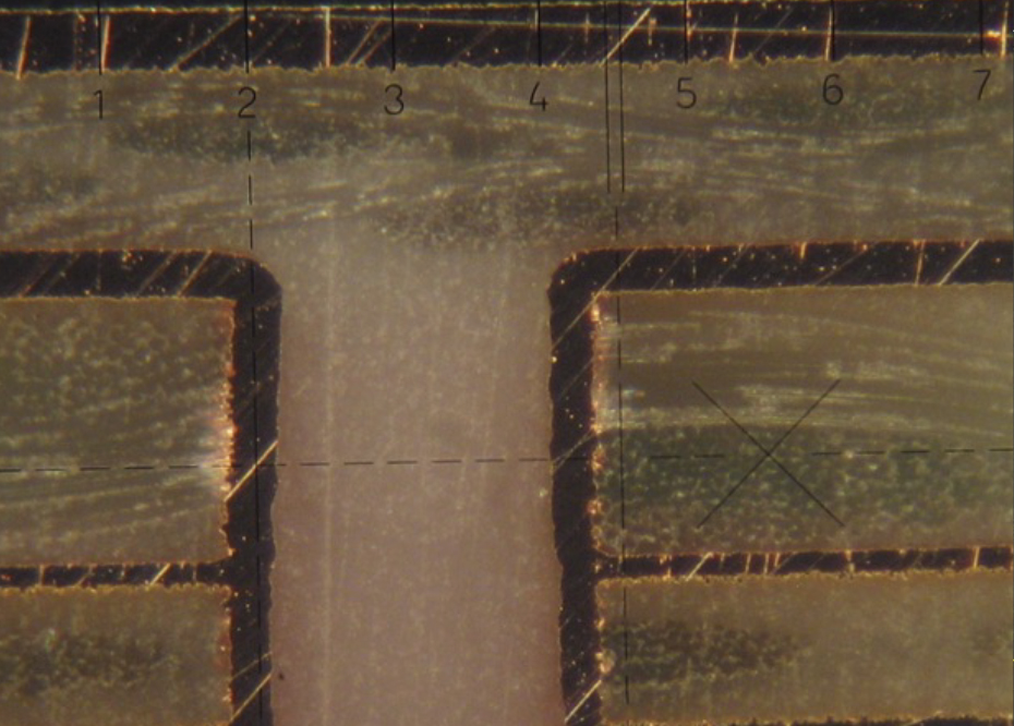
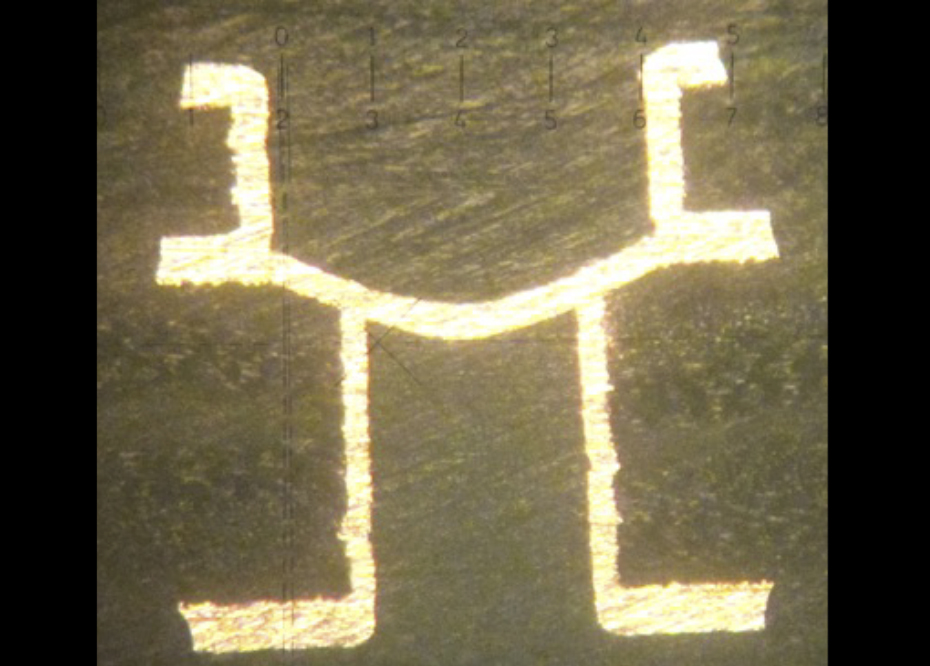
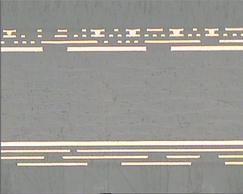
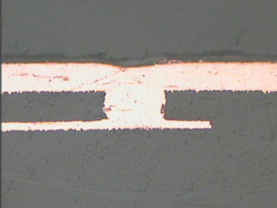
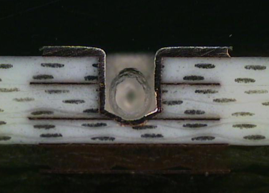
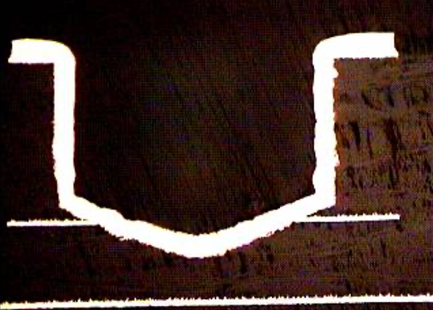
Drilling and subsequent copper plating of the via walls allows different layers of the PCB to be interconnected.
With increasing performance, there is an increasing number of interconnections to achieve, for which it is increasingly necessary to design PCBs with blind vias, obtained by laser drilling or mechanical drilling, or buried or with a combination of both these drilling solutions. This is why the drilling process must ensure the highest quality. The better the drilling process, the higher the quality of the copper plating and therefore also the signal integrity.
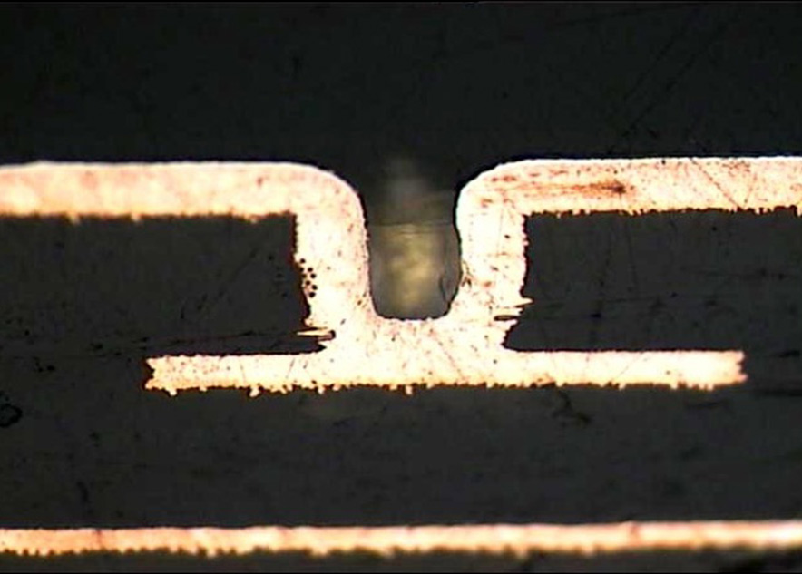
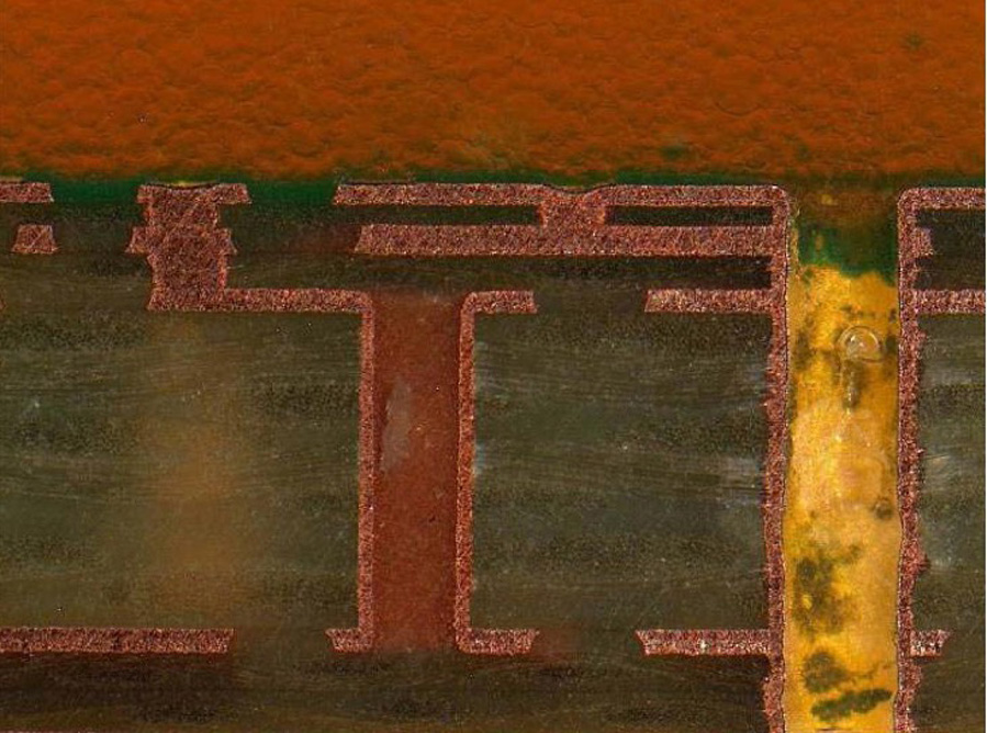
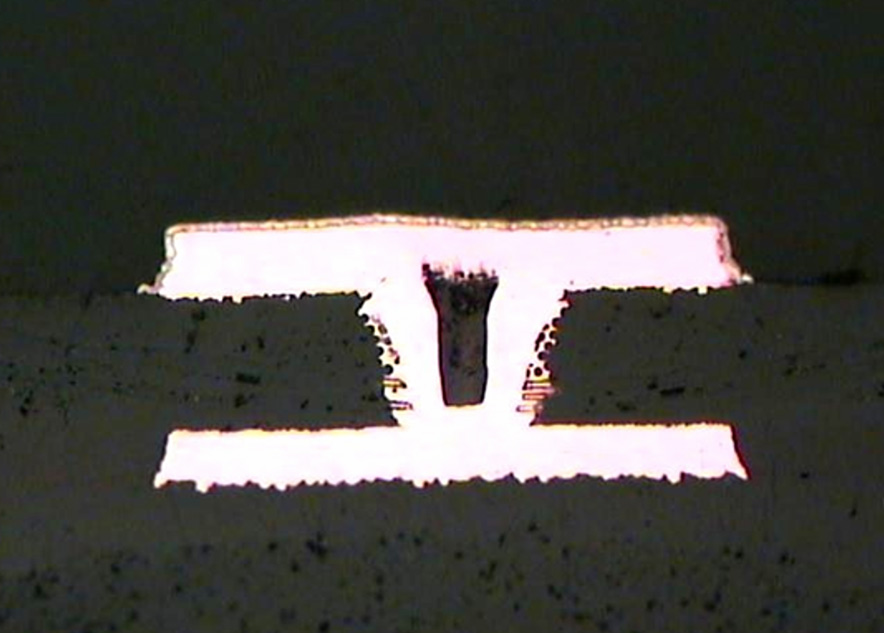
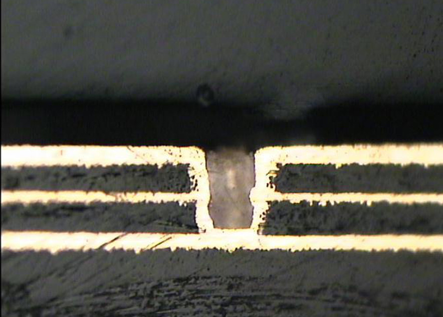
At the same time, we are witnessing the evolution of via filling techniques associated with these drilling processes, including copper filling and resin filling, using conductive or non-conductive resins, with and without vacuum application.
The demand for these drilling techniques and the related filling process is growing rapidly as it responds to the need to produce ever higher-performing electronic devices, including PCBs.
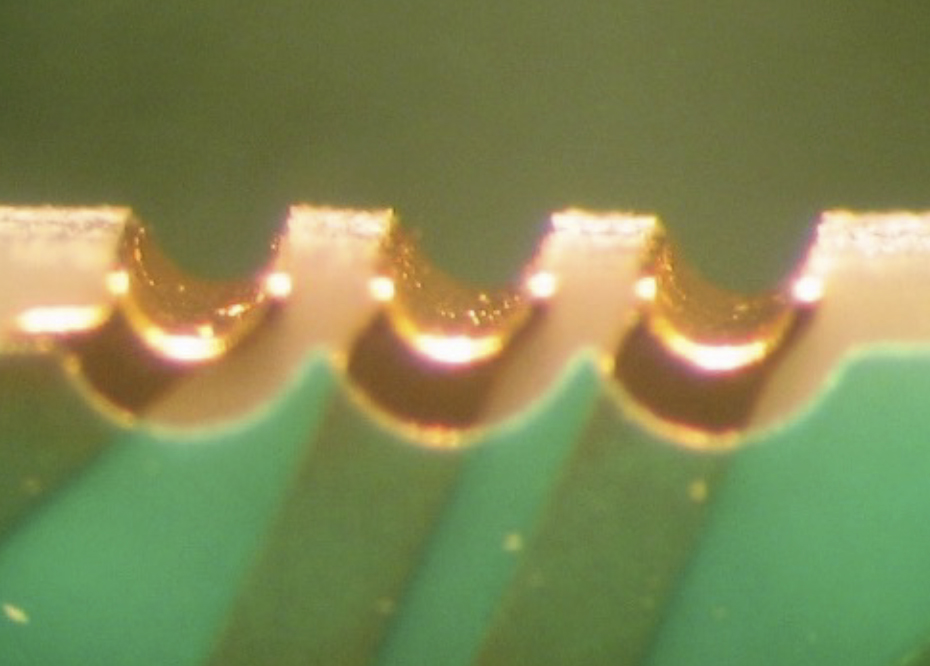
This is the case of the HDI PCB. Here the microvias can be a via-in-pad type for mounting components, staggered or stacked, subsequently filled with non-conductive resins - resin filling - and plated with copper at the top or filled with copper - copper filling - and plated with copper to obtain filled and capped vias.
Reverse build-up technology can also be used to ensure that the pads are perfectly level.
Rely on us to find the right solution for your PCB.