Lab analysis & product certification
Product and process quality analysis, our labs

Having the appropriate instruments is essential in order to ensure full compliance with the technical specifications and design characteristics of the PCBs in accordance with increasingly stringent quality standards and requirements.
The instruments required in particular must be capable of supporting the Statistical Process Control (SPC) and the ensuing PCB analysis.
Today, carrying out the necessary checks and assessments is essential to ensure the conformity of printed circuit boards throughout the life cycle of the product they will be part of, regardless of the scope and the market sector in which they are used.

It has thus become necessary to adopt the most advanced laboratory technologies in order to ensure compliance with the international standards in use in the manufacturing of electronic products and with specific requirements expressed by the end customer.
International standards, first and foremost the IPC standards, in particular suggest developing a collaboration between designers (representatives of the end consumer in general), manufacturers and assemblers of printed circuit boards to minimise the criticalities of the printed circuit and electronic components assembly system (PCBA) and, more generally, of the finished product.
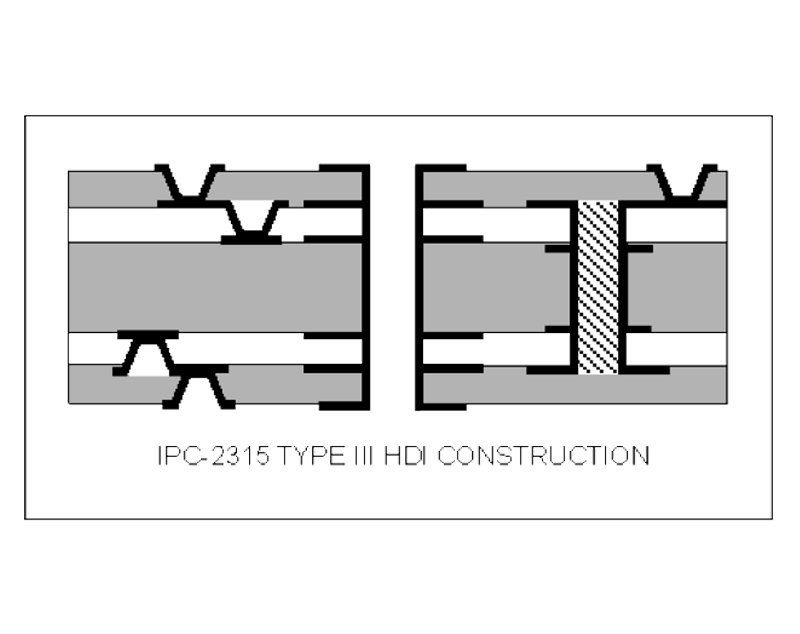
Microvias are used to check the internal characteristics (i.e. thickness of copper deposit on the walls of vias and for the assessment of the most critical points such as the corners of PTH holes and vias holes or the annular ring near the interconnections between the hole and inner layers.
Another key aspect is to check the construction stack-up, above all, but not only, for controlled impedance circuits. The microvia allows you to assess the presence and thickness of all the layers envisaged, as well as to assess the thickness of the base copper in the inner layers and the subsequent chemical copper and electrolytic copper fillings.
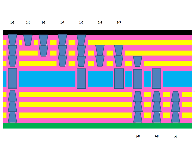
The controlled impedances are calculated during the development of the PCB by the designers, based on the material chosen to manufacture it, and then checked again and simulated during the feasibility and engineering study, according to the material definitively shared with the same designer. The dielectric constant of the base laminate together with the sizing of the impedance traces determine the value of the controlled impedances.
The impedance levels can be measured using dedicated test coupons inserted in the manufacturing equipment to ensure that they are as representative as possible of the actual PCBs.
More complex structures with increasing drilling densities make PCBs more susceptible to thermal stresses, particularly during the soldering processes of electronic components.
For this reason, thermal stress tests are essential to simulate the behaviour of the PCBs and their robustness during the soldering process in the reflow oven immediately after the placement of the SMD components operated with pick & place machines.
Thermal stresses are applied to check the metallization resistance of PTH holes: in accordance with IPC TM650 standards, they are applied with 3 stresses at 288°C (IPC TM 650 2.6.8), or the reflow process is simulated with 6 stresses at 260°C (IPC TM650 2.6.27).
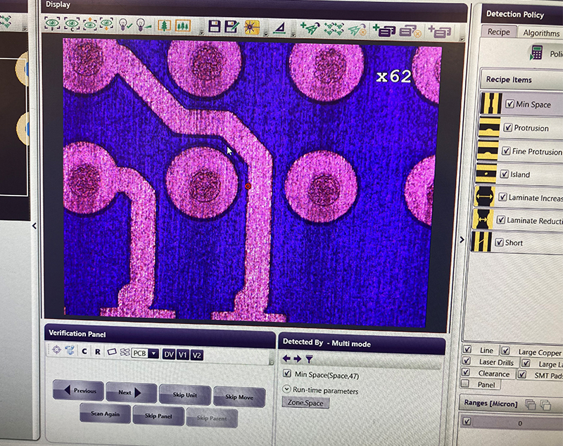
The destructive analyses, in other words those which render the PCB unusable and which are often necessary to investigate the characteristics the PCB derives from the special manufacturing processes, are supplemented with non-destructive analyses.
One example is the X-Ray Fluorescence Spectroscopy (XRF) analysis to determine the thickness of the surface finishes.
The surface finish thickness analysis not only checks the conformity of the printed circuit board, but also allows the finish processes to be kept under control.
Indeed, finish thicknesses that fail to comply with IPC standards could create a number of issues during the component soldering process.
The product analysis results are collected in commonly used documents to certify product conformity, such as: CoC, FAI Report, PPAP, Test Report prepared according to any specific requests made by the customer.
We certify the quality PCB by relying on the finest lab technologies.