HDI / Sequential build up (SBU) PCBs
HDI Printed Circuit Boards / Sequential build up (SBU)

The acronym HDI stands for "High Density Interconnections".
The increase in density of interconnections which has already taken place with the development of multi-layer PCBs has been exasperated in HDI printed circuit boards, where the performance-space ratio has been maximised.
For the same number of interconnections, an HDI PCB has a smaller amount of layers compared to a traditional multi-layer circuit board.
In HDI printed circuit boards, the width of the traces is reduced, as are both the size and density of pads per surface area unit. Laser drilling becomes a key technology to increase the number of interconnections between the layers of copper.
An HDI circuit can be made via several configurations and, in particular, through a sequential build-up process where each pressing level corresponds to a specific drilling phase.
The HDI structures are described by the IPC-2513.
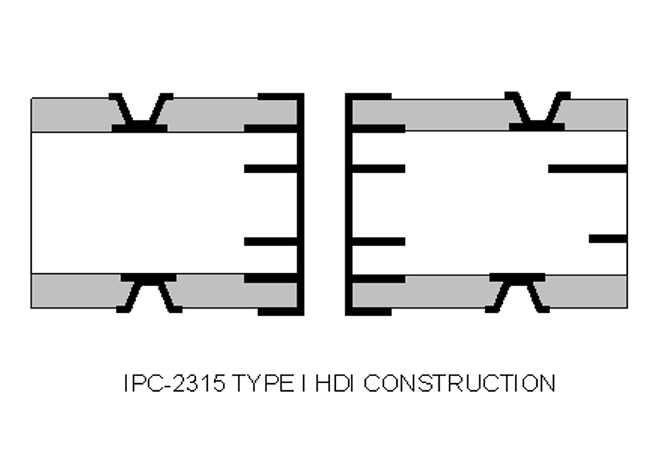
HDI TYPE I construction
In this case, both blind laser and through hole vias are envisaged.
Blind laser vias can be found on just one or on both the external sides.
Buried vias are not envisaged.
The number of layers is variable, though it should be limited to contain the ratio of the plated through hole vias.
TYPE II
TYPE II construction envisages laser blind vias, buried vias and through hole vias.
Laser blind vias can be found on just one or on both the external sides, stacked on buried vias or staggered.
Buried vias connect layer 2 with layer n-1, where 1 and n are the external layers of the printed circuit, and must be filled during the pressing phase with the resin contained in the pre-preg or through the silk screen-printing process with epoxy resin.
For TYPE II constructions too, it is advisable for the number of layers to be limited to limit the ratio of plated through hole vias.
Nevertheless, using buried vias allows you to reduce the number of layers in the printed circuit and thus also reduce the diameter of the through hole vias, although it won’t reduce the width of the traces.
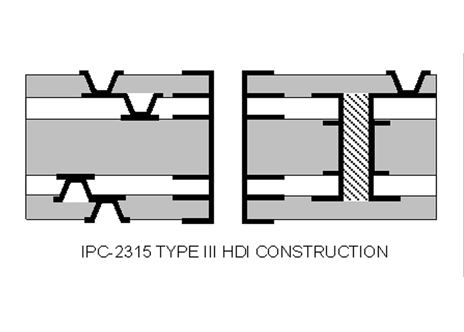
TYPE III
TYPE III constructions envisage buried vias and laser blind vias with at least two HDI layers on one or both sides of the printed circuit board.
Laser vias can be stacked or staggered with respect to one another or stacked and staggered with respect to the buried vias.
The greater number of interconnections assured by this type of construction means the diameter of through hole vias and the width of the traces can be reduced.
In the event that plated through hole vias are used, then the restrictions pointed out for the previous two construction types also apply.
This construction is among the most frequently used because it gives PCB designers greater freedom of design.
At EPN we produce printed circuit boards with Type I and Type II structures to meet the majority of market demands.
Where required, to fill the holes we use copper filling and resin filling treatments, using both conductive and non-conductive resins.
We have the expertise and the technology also to produce filled & capped vias in order further to optimise the management of space on the printed circuit board.