From activation to photoprinting of the innerlayers
Lamination and photo printing process
As reported in our first article, examining a basic cycle of a Multilayer product, the processes of
1. activation and lamination of innerlayers and
2. photoprinting of the innerlayers
correspond to the first two production steps.
The inner layer represents one of the most important base materials for the realization of a multilayer PCB given that it is part of the build-up of the PCB itself.
It is a foil of variable thickness, consisting of three layers of which:
- the central one is made up of a glass fiber fabric pre-impregnated with thermosetting resin and
- the two external layers are represented by two copper foils.
The thicknesses of both, the central layer and the two external copper foils, can vary according to project needs and functional specifications required from each PCB.
Inner layers’ central layer is generally FR4 (flame retardant 4) material, however, the type of resin and the glass fiber can have different characteristics giving each PCB mechanical and electrical properties suitable for each specific application. It is important to know that different materials have significantly different costs, and, for this reason, the choice must be guided by actual needs.
PCBs manufacturing process begins with the processing of the inners, which are chemically treated, the external copper surfaces are activated by micro-etching to increase their roughness and to ensure better adhesion of the dry film, a photosensitive cellulose film that is applied on both sides of the innerlayer through a process called lamination.
You can choose among different type of dry film according to the characteristics of the inner copper thickness and of the nets drawing that will be printed in the photoprinting phase, which consists in exposing the dry film itself to a light source.
There are two different photoprinting techniques:
- the reverse imaging, typical of traditional photography, and
- the direct imaging, made through laser or LED systems (Laser Direct Imaging and Led Direct Imaging).
Reverse imaging photo printing
In the first case it is necessary to print the negative of the nets drawing expected by gerber on a specific slide through a machine called plotter. This film will then be used in a photo printing machine where it will be interposed between a light source and the dry-film laminated on the inner: each time the light source emits light, the positive of the nets drawing is "photographed" on the dry-film itself. The characteristics of the dry-film hit by the light change, it becomes more resistant (in fact it polymerizes) and this will allow the underlying copper to be preserved in the subsequent development phases (removal of the uncured dry-film), this means that the copper tracks provided by gerber are preserved. All dry film on the remaining part of the panel and the underlying copper will instead be removed in specific phases that are called dry-film development, Copper etching and dry-film stripping.
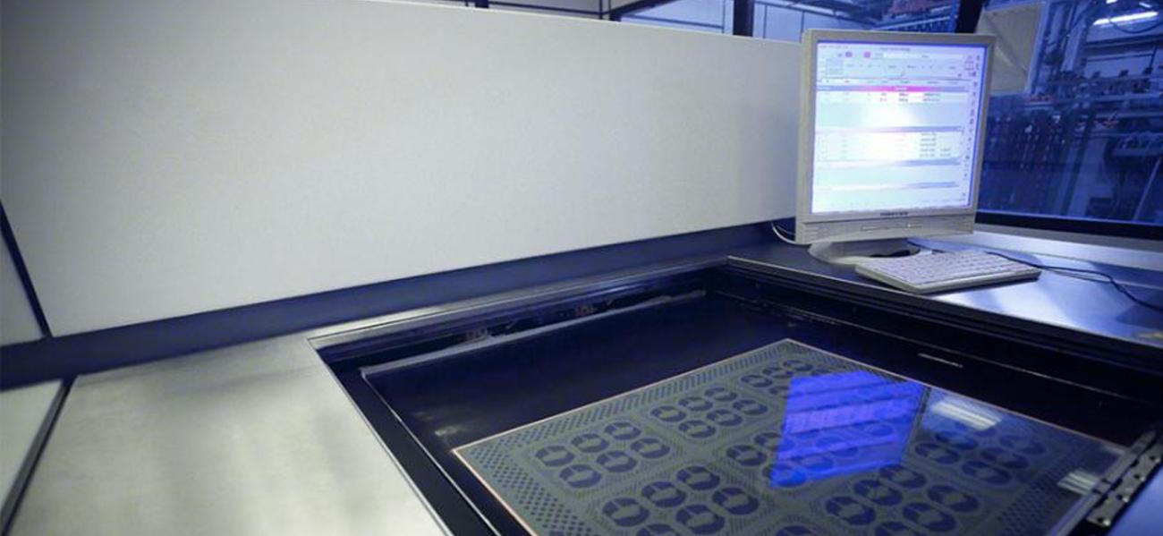
Direct imaging photo printing
In this case, the dry film is selectively struck to draw the nets expected by gerber by a beam of laser light or by a beam of LED light, two different technologies for the same imaging technique.
The advantages of “direct imaging” are numerous:
- a plotted slide, which is in fact a consumable, is not required;
- a plotter (and relative developer) and a technician capable of programming it as well as one capable of using it are not required;
- the plotted slide is subject to aging, this means that it changes size (length variation on x and y axis), over the time and to limit this effect it is necessary to store it in an ad hoc environment with controlled temperature and humidity conditions;
- in any case, for this reason, a new slide must be periodically re-plotted;
- an error on the plotted slide, generated by a scratch or more commonly by a particle of dust, is transmitted to all the inners that have foreseen its use;
- the plotted slide does not allow ad hoc adaptations: “indirect printing” does not allow corrections based on the distortions of each individual inner.
Traditional reverse printing has therefore been outdated by direct imaging technologies which, in addition, allow to guarantee, with maximum precision, the creation of copper nets and insulations tracks of significantly lower thickness, even below 50 microns.
We will continue describing the process in the next articles, meanwhile, to explain how many and how deep is the knowledge requested to operate in the PCBs production, we’d like to point out that even considering only these first phases of the process we already introduced notions relating to basic materials, organic and inorganic chemistry as well as relating to photoprinting.
It is also necessary to highlight that the acceleration in the development of electronic devices with increased performance has imposed a similar acceleration in the development of the technologies for manufacturing.
Therefore, to manufacture PCBs, it is necessary not only to have numerous machineries, but always to have those that are updated with the latest technologies. You snooze you lose!